25. January 2018
Schematic Symbols that make sense
Some people draw their schematic symbols strait according to the pin arrangement of the component.
For explanation they say this prevents confusion during layout when signals are on a different location then in the schematic.
But the schematic is the “Source code” for the layout design. It needs to be drawn in a way to be read fast and unambiguously to enable that mistakes in connections can be spotted easily. For this it helps to prevent wire crossings where ever possible.
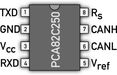
As an example here a CAN-Transceiver with only 8 pins:
The “simple” approach placing the pins for the schematic symbol like on the physical part, leads even for this small device to a surprisingly unreadable schematic:
The approach optimized for schematic leads to a much more easily readable and cleaner schematic without wire crossings:


